| |
Metal-to-semiconductor
contacts are of great importance since they are present in every
semiconductor device. They can behave either as a Schottky barrier or as
an ohmic contact dependent on the characteristics of the interface. This
chapter contains an analysis of the electrostatics of the M-S junction
(i.e. the charge, field and potential distribution within the device)
followed by a derivation of the current voltage characterisitics due to
diffusion, thermionic emission and tunneling and a discussion of the
non-ideal effects in Metal-Semiconductor junctions.
Structure and principle of operation |
|
1. Structure
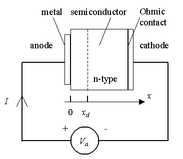
The structure of a metal-semiconductor junction is shown in
Figure 1. It consists of a metal contacting a piece of
semiconductor. An ideal Ohmic contact, a contact such that no
potential exists between the metal and the semiconductor, is made to
the other side of the semiconductor. The sign convention of the
applied voltage and current is also shown on Figure 1.
|
|

Figure 1 : Structure and sign
convention of a metal-semiconductor
junction |
2. Flatband diagram and built-in
potential |
|
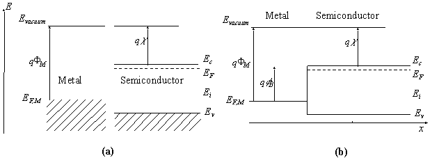
| The barrier between the metal and the semiconductor
can be identified on an energy band diagram. To construct such
diagram we first consider the energy band diagram of the metal and
the semiconductor, and align them using the same vacuum level as
shown in Figure 2 (a). As the metal and semiconductor are brought
together, the Fermi energies of the metal and the semiconductor do
not change right away. This yields the flatband diagram of Figure 2
(b). |
|
Figure 2 :
|
Energy band diagram of the metal
and the semiconductor before (a) and after (b) contact is
made. |
| The barrier height, fB, is defined as the potential
difference between the Fermi energy of the metal and the band edge
where the majority carriers reside. From Figure 2 (b) one finds that
for an n-type semiconductor the barrier height is obtained
from: |
 |
(1.1) |
| Where FM is the
work function of the metal and c is the
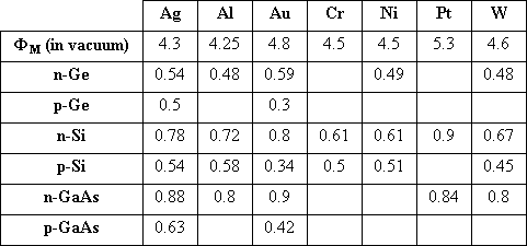
electron affinity. The work function of selected metals as measured
in vacuum can be found in Table 1.
For p-type material, the barrier height is given by the difference
between the valence band edge and the Fermi energy in the
metal: |
 |
(1.2) |
| A metal-semiconductor junction will therefore form a
barrier for electrons and holes if the Fermi energy of the metal as
drawn on the flatband diagram is somewhere between the conduction
and valence band edge. |
| In addition, we define the built-in potential, fI, as the difference between the
Fermi energy of the metal and that of the semiconductor.
|
 |
(1.3) |
 |
(1.4) |
| The measured barrier height for selected
metal-semiconductor junctions is listed in Table 1.
These experimental barrier heights often differ from the ones
calculated using (1.1) or (1.2). This is due to the detailed behavior of the
metal-semiconductor interface. The ideal metal-semiconductor theory
assumes that both materials are infinitely pure, that there is no
interaction between the two materials nor is there an interfacial
layer. Chemical reactions between the metal and the semiconductor
alter the barrier height as do interface states at the surface of
the semiconductor and interfacial layers. Some general trends
however can still be observed. As predicted by (1.1), the barrier height on n-type semiconductors
increases for metals with a higher work function as can be verified
for silicon. Gallium arsenide on the other hand is known to have a
large density of surface states so that the barrier height becomes
virtually independent of the metal. Furthermore, one finds the
barrier heights reported in the literature to vary widely due to
different surface cleaning procedures. |
| Table 1: Workfunction of selected
metals and their measured barrier height on Ge, Si and
GaAs. |
|

|
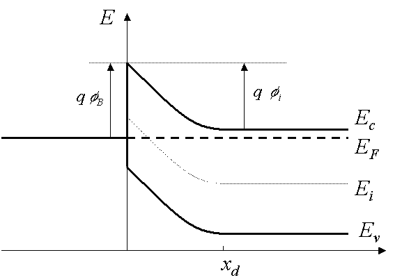
| The flatband diagram, shown in Figure 2
(b), is not a thermal equilibrium diagram, since the Fermi energy in
the metal differs from that in the semiconductor. Electrons in the
n-type semiconductor can lower their energy by traversing the
junction. As the electrons leave the semiconductor, a positive
charge, due to the ionized donor atoms, stays behind. This charge
creates a negative field and lowers the band edges of the
semiconductor. Electrons flow into the metal until equilibrium is
reached between the diffusion of electrons from the semiconductor
into the metal and the drift of electrons caused by the field
created by the ionized impurity atoms. This equilibrium is
characterized by a constant Fermi energy throughout the structure.
|
|
Figure 3
: |
Energy band diagram of a
metal-semiconductor contact in thermal
equilibrium. |
| It is of interest to note that in thermal
equilibrium, i.e. with no external voltage applied, there is a
region in the semiconductor close to the junction ( ), which is
depleted of mobile carriers. We call this the depletion region. The
potential across the semiconductor equals the built-in potential,
fi. |
2.4. Forward and reverse bias |
|
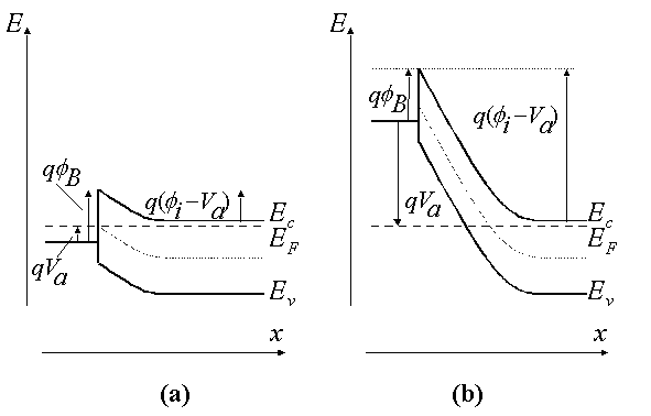
| Operation of a metal-semiconductor junction under
forward and reverse bias is illustrated with Figure 4. As a positive
bias is applied to the metal (Figure 4 (a)), the Fermi energy of the
metal is lowered with respect to the Fermi energy in the
semiconductor. This results in a smaller potential drop across the
semiconductor. The balance between diffusion and drift is disturbed
and more electrons will diffuse towards the metal than the number
drifting into the semiconductor. This leads to a positive current
through the junction at a voltage comparable to the built-in
potential. |
|
Figure 4
: |
Energy band diagram of a
metal-semiconductor junction under (a) forward and (b) reverse
bias |
| As a negative voltage is applied (Figure 4 (b)), the
Fermi energy of the metal is raised with respect to the Fermi energy
in the semiconductor. The potential across the semiconductor now
increases, yielding a larger depletion region and a larger electric
field at the interface. The barrier, which restricts the electrons
to the metal, is unchanged so that the flow of electrons is limited
by that barrier independent of the applied voltage. The
metal-semiconductor junction with positive barrier height has
therefore a pronounced rectifying behavior. A large current exists
under forward bias, while almost no current exists under reverse
bias. |
| The potential across the semiconductor therefore
equals the built-in potential, fi, minus the applied voltage,
Va. |
 |
(2.1) |
3. Electrostatic analysis
3.1. General discussion - Poisson's
equation |
|
| The electrostatic analysis of a metal-semiconductor
junction is of interest since it provides knowledge about the charge
and field in the depletion region. It is also required to obtain the
capacitance-voltage characteristics of the
diode. |
| The general analysis starts by setting up Poisson's
equation: |
 |
(3.1) |
| where the charge density, r,
is written as a function of the electron density, the hole density
and the donor and acceptor densities. To solve the equation, we have
to express the electron and hole density, n and p, as
a function of the potential, f, yielding:
|
 |
(3.2) |
 |
(3.3) |
| where the potential is chosen to be zero in the
n-type region, where x >>
xn. |
| This second-order non-linear differential equation
(3.2) can not be solved analytically. Instead we will make the
simplifying assumption that the depletion region is fully depleted
and that the adjacent neutral regions contain no charge. This full
depletion approximation is the topic of section 3.2.
|
3.2. Full depletion approximation |
|
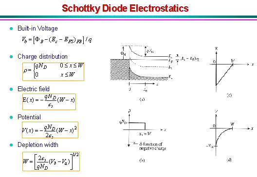
| The simple analytic model of the metal-semiconductor
junction is based on the full depletion approximation. This
approximation is obtained by assuming that the semiconductor is
fully depleted over a distance xd, called the
depletion region. While this assumption does not provide an accurate
charge distribution, it does provide very reasonable approximate
expressions for the electric field and potential throughout the
semiconductor. |
3.3. Full depletion analysis |
|
| We now apply the full depletion approximation to an
M-S junction containing an n-type semiconductor. We define the
depletion region to be between the metal-semiconductor interface
(x = 0) and the edge of the depletion region (x =
xd). The depletion layer width,
xd, is unknown at this point but will later be
expressed as a function of the applied voltage. |
| To find the depletion layer width, we start with the
charge density in the semiconductor and calculate the electric field
and the potential across the semiconductor as a function of the
depletion layer width. We then solve for the depletion layer width
by requiring the potential across the semiconductor to equal the
difference between the built-in potential and the applied voltage,
fi - Va. The
different steps of the analysis are illustrated by Figure
3.1. |
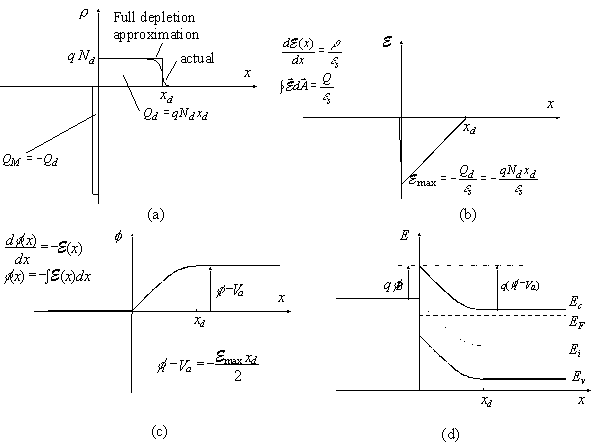
| As the semiconductor is depleted of mobile carriers
within the depletion region, the charge density in that region is
due to the ionized donors. Outside the depletion region, the
semiconductor is assumed neutral. This yields the following
expressions for the charge density, r:
|
 |
(3.3.4) |
| where we assumed full ionization so that the ionized
donor density equals the donor density, Nd. This
charge density is shown in Figure 3.1 (a). The charge in the
semiconductor is exactly balanced by the charge in the metal,
QM, so that no electric field exists except around
the metal-semiconductor interface. |
| Figure 3.1
: |
(a) Charge density, (b) electric
field, (c) potential and (d) energy as obtained with the full
depletion analysis. |
| Using Gauss's law we obtain electric field as a
function of position, also shown in Figure 3.1 (b):
|
 |
(3.5) |
| where es is the
dielectric constant of the semiconductor. We also assumed that the
electric field is zero outside the depletion region. It is expected
to be zero there since a non-zero field would cause the mobile
carriers to redistribute until there is no field. The depletion
region does not contain mobile carriers so that there can be an
electric field. The largest (absolute) value of the electric field
is obtained at the interface and is given by: |
 |
(3.6) |
| where the electric field was also related to the
total charge (per unit area), Qd, in the depletion
layer. Since the electric field is minus the gradient of the
potential, one obtains the potential by integrating the expression
for the electric field, yielding: |
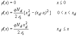 |
(3.7) |
| We now assume that the potential across the metal can
be neglected. Since the density of free carriers is very high in a
metal, the thickness of the charge layer in the metal is very thin.
Therefore, the potential across the metal is several orders of
magnitude smaller that that across the semiconductor, even though
the total amount of charge is the same in both
regions. |
| The total potential difference across the
semiconductor equals the built-in potential, fi, in thermal equilibrium and is
further reduced/increased by the applied voltage when a
positive/negative voltage is applied to the metal as described by
equation (3.2.5). This boundary condition provides the following
relation between the semiconductor potential at the surface, the
applied voltage and the depletion layer width: |
 |
(3.8) |
| Solving this expression for the depletion layer
width, xd, yields: |
 |
(3.9) |
3.4. Junction capacitance |
|
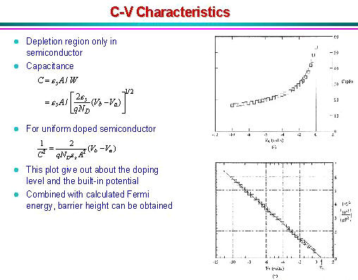
| In addition, we can obtain the capacitance as a
function of the applied voltage by taking the derivative of the
charge with respect to the applied voltage yielding:
|
 |
(3.10) |
| The last term in the equation indicates that the
expression of a parallel plate capacitor still applies. One can
understand this once one realizes that the charge added/removed from
the depletion layer as one decreases/increases the applied voltage
is added/removed only at the edge of the depletion region. While the
parallel plate capacitor expression seems to imply that the
capacitance is constant, the metal-semiconductor junction
capacitance is not constant since the depletion layer width,
xd, varies with the applied voltage.
|
3.5. Schottky barrier lowering |
|
| Image charges build up in the metal electrode of a
metal-semiconductor junction as carriers approach the
metal-semiconductor interface. The potential associated with these
charges reduces the effective barrier height. This barrier reduction
tends to be rather small compared to the barrier height itself.
Nevertheless this barrier reduction is of interest since it depends
on the applied voltage and leads to a voltage dependence of the
reverse bias current. Note that this barrier lowering is only
experienced by a carrier while approaching the interface and will
therefore not be noticeable in a capacitance-voltage measurement.
|
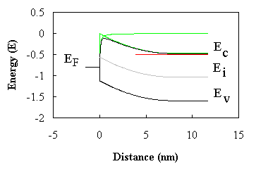
| An energy band diagram of an n-type silicon Schottky
barrier including the barrier lowering is shown in Figure 3.2:
|
| Figure 3.2: |
Energy band diagram of a silicon Schottky barrier
with fB = 0.8 V and
Nd = 1019
cm-3. |
| Shown is the energy band diagram obtained using the
full-depletion approximation, the potential reduction experienced by
electrons, which approach the interface and the resulting conduction
band edge. A rounding of the conduction band edge can be observed at
the metal-semiconductor interface as well as a reduction of the
height of the barrier. |
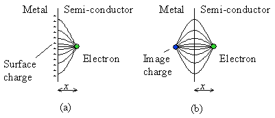
| The calculation of the barrier reduction assumes that
the charge of an electron close to the metal-semiconductor interface
attracts an opposite surface charge, which exactly balances the
electron's charge so that the electric field surrounding the
electron does not penetrate beyond this surface charge. The time to
build-up the surface charge and the time to polarize the
semiconductor around the moving electron is assumed to be much
shorter than the transit time of the electron . This scenario is
based on the assumption that there are no mobile or fixed charges
around the electron as it approaches the metal-semiconductor
interface. The electron and the induced surface charges are shown in
Figure 3.3: |
| Figure
3.3: |
a) Field lines and surface
charges due to an electron in close proximity to a perfect conductor
and b) the field lines and image charge of an electron.
|
| It can be shown that the electric field in the
semiconductor is identical to that of the carrier itself and another
carrier with opposite charge at equal distance but on the opposite
side of the interface. This charge is called the image charge. The
difference between the actual surface charges and the image charge
is that the fields in the metal are distinctly different. The image
charge concepts is justified on the basis that the electric field
lines are perpendicular to the surface a perfect conductor, so that,
in the case of a flat interface, the mirror image of the field lines
provides continuous field lines across the interface.
|
| The barrier lowering depends on the square root of
the electric field at the interface and is calculated
from: |
 |
(3.11) |
4. Schottky diode current
| The current across a metal-semiconductor junction is
mainly due to majority carriers. Three distinctly different
mechanisms exist: diffusion of carriers from the semiconductor into
the metal, thermionic emission of carriers across the Schottky
barrier and quantum-mechanical tunneling through the barrier. The
diffusion theory assumes that the driving force is distributed over
the length of the depletion layer. The thermionic emission theory on
the other hand postulates that only energetic carriers, those, which
have an energy equal to or larger than the conduction band energy at
the metal-semiconductor interface, contribute to the current flow.
Quantum-mechanical tunneling through the barrier takes into account
the wave-nature of the electrons, allowing them to penetrate through
thin barriers. In a given junction, a combination of all three
mechanisms could exist. However, typically one finds that only one
limits the current, making it the dominant current
mechanism. |
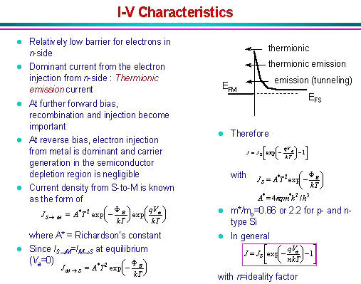
| The analysis reveals that the diffusion and
thermionic emission currents can be written in the following
form: |
 |
(4.1) |
| This expression states that the current is the
product of the electronic charge, q, a velocity, v,
and the density of available carriers in the semiconductor located
next to the interface. The velocity equals the mobility multiplied
with the field at the interface for the diffusion current and the
Richardson velocity (see section 3.4.2)
for the thermionic emission current. The minus one term ensures that
the current is zero if no voltage is applied as in thermal
equilibrium any motion of carriers is balanced by a motion of
carriers in the opposite direction. |
| The tunneling current is of a similar form,
namely: |
 |
(4.2) |
| where vR is the Richardson velocity
and n is the density of carriers in the semiconductor. The
tunneling probability term, Q, is added
since the total current depends on the carrier flux arriving at the
tunnel barrier multiplied with the probability, Q, that they tunnel through the barrier.
|
| This analysis assumes that the depletion layer is
large compared to the mean free path, so that the concepts of drift
and diffusion are valid. The resulting current density
equals: |
 |
(4.3) |
The current therefore depends exponentially on the
applied voltage, Va, and the barrier height, fB. The prefactor can more easily be
understood if one rewrites it as a function of the electric field at
the metal-semiconductor interface,  max: max: |
 |
(4.4) |
 |
(4.5) |
| so that the prefactor equals the drift current at the
metal-semiconductor interface, which for zero |
| The thermionic emission theory assumes that
electrons, which have an energy larger than the top of the barrier,
will cross the barrier provided they move towards the barrier. The
actual shape of the barrier is hereby ignored. The current can be
expressed as: |
 |
(4.6) |
where  is the Richardson constant and fB is the Schottky barrier
height. is the Richardson constant and fB is the Schottky barrier
height. |
| The expression for the current due to thermionic
emission can also be written as a function of the average velocity
with which the electrons at the interface approach the barrier. This
velocity is referred to as the Richardson velocity given
by: |
 |
(4.7) |
| So that the current density
becomes: |
 |
(4.8) |
| The tunneling current is obtained from the product of
the carrier charge, velocity and density. The velocity equals the
Richardson velocity, the velocity with which on average the carriers
approach the barrier. The carrier density equals the density of
available electrons, n, multiplied with the tunneling
probability, Q,
yielding: |
 |
(4.9) |
| Where the tunneling probability is obtained
from: |
 |
(4.10) |
and the electric field equals  = fB/L. = fB/L. |
| The tunneling current therefore depends exponentially
on the barrier height, fB, to
the 3/2 power. |
Bibliography
- Physics of Semiconductor Devices, Second edition, S. M. Sze, Wiley
& Sons, 1981, Chapter 5.
- Device Electronics for Integrated Circuits, Second edition, R.S.
Muller and T. I. Kamins, Wiley & Sons, 1986, Chapter 3.
SCHOTTKY DIODES
Metal-semiconductor
contact at zero bias
Electrons in the conduction band of a
crystal can be viewed as sitting in a potential box formed by the crystal
boundaries (see Fig. 1). This potential box for electrons is
usually deeper in a metal than in a semiconductor. If a metal
and a semiconductor are brought together into a close proximity, some
electrons from the metal will move into the semiconductor and some
electrons from the semiconductor will move into the metal. However,
since the barrier for the electron escape from the metal is higher, more
electrons will transfer from the semiconductor into the metal than in the
opposite direction. At thermal equilibrium, the metal will be charged
negatively, and the semiconductor will be charged positively, forming a
dipole layer that is very similar to that in a p+-n
junction. The Fermi level will be constant throughout the entire
metal-semiconductor system, and the energy band diagram in the
semiconductor will be similar to that for an n-type semiconductor
in a p+-n junction (see Fig.
2).

Fig.
1. Schematic
energy diagram for electrons in conduction bands of a metal and of a
semiconductor.
Energies
Fm and
Fs
shown in Fig. 2 are called the metal and the semiconductor work
functions. The work function is equal to the
difference between the vacuum level (which is defined as a free electron energy in vacuum) and the Fermi
level. The electron affinity of the semiconductor,
Cs
(also shown in Fig. 2), corresponds to the energy separation between the
vacuum level and the conduction band edge of the semiconductor.

Fig.
2. Simplified energy diagram
of GaAs metal-semiconductor barrier q
fb is the barrier
height (0.75 eV), Cs is the
electron affinity in the semiconductor, Fs and
Fm are
the semiconductor and the metal work functions, and
Vbi (0.591
V) is the built-in voltage. Donor concentration in GaAs is 1015
cm–3.
A metal-semiconductor diode is called a
Schottky diode. In the
idealized picture of the Schottky
junction shown in Fig. 2, the energy barrier between the
semiconductor and the metal is
 (1)
(1)
Since Fm > Fs the
metal is charged negatively. The positive net space charge in the
semiconductor leads to a band bending
 (2)
(2)
where Vbi is called the
built-in voltage, in analogy with the corresponding quantity in a
p-n junction. Note that qVbi is also identical to the
difference between the Fermi levels in the metal and the semiconductor
when separated by a large distance (no exchange of charge); see Fig.
1.
However, eq.
(1) and Fig. 2 are not quite
correct. In reality, a change in the metal work function,
Fm, is not
equal to the corresponding change in the barrier height
,fb, as
predicted by eq. (1). In actual Schottky diodes,
fb
increases with an increase in Fm but only by 0.1 to 0.3 eV
when Fm increases by
1 to 2 eV. Even though a detailed and
accurate understanding of Schottky barrier
formation remains a challenge, many properties of Schottky barriers may be understood independently of
the exact mechanism determining the barrier height. In other words,
we can simply determine the effective barrier height from experimental
data. Usually, as a crude and empirical rule of thumb, we can assume
that the Schottky barrier height for an
n-type semiconductor is close to 1/2 and 2/3 of the energy gap.
In a Schottky
diode, the semiconductor band diagram looks very similar to that of an
n-type semiconductor in a p+-n
diode (compare Fig. 1a and 2). Hence,
the variation of the space charge density, r, the electric field,
F, and the potential, f, in the
semiconductor near the metal-semiconductor interface can be found using
the depletion approximation:
 (3)
(3)
 (4)
(4)
 (5)
(5)
(Here
x = 0 corresponds to the metal-semiconductor
interface.) The depletion layer width, xn, at
zero bias is given by
 (6)
(6)
Schottky diode under bias
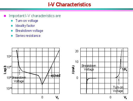
Forward bias corresponds to a positive
voltage applied to the metal with respect to the semiconductor.
Just as for a p+-n junction, the
depletion width under small forward bias and reverse
bias may be obtained by substituting Vbi with
Vbi– V, where V is the applied
voltage. As illustrated in Fig. 3, the application of a
forward bias decreases the potential barrier for electrons moving from the
semiconductor into the metal. Hence, the current-voltage
characteristic of a Schottky diode can be
described by a diode equation, similar to that for a p-n
junction diode :
 (7)
(7)
where Is is the saturation
current, Rsis the series resistance,
Vth =
kBT/q is the thermal voltage, and h is the ideality
factor (h typically varies from 1.02 to 1.6).
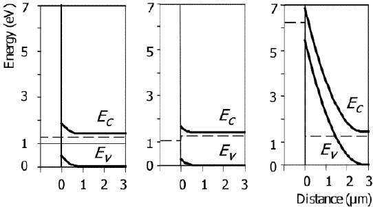 (a)
(b)
(c)
Fig. 3.
Band diagrams for a GaAs Schottky barrier diode
at (a) zero bias, (b) 0.2 V forward bias, and (c) 5 V reverse bias.
Dashed line shows the position of the Fermi level in the metal (x
< 0) and in the semiconductor (x
> 0).
Thermionic emission.
The diode saturation current,
Is, is typically much
larger for Schottky barrier diodes than in
p-n junction diodes since the Schottky
barrier height is smaller than the barrier height in p-n junction
diodes. In a p-n junction, the height of the barrier
separating electrons in the conduction band of the n-type region
from the bottom of the conduction band in the p-region is on the order of the energy gap. A typical Schottky barrier height is only about two thirds of
the energy gap or less, as mentioned above. Also, the mechanism of the electron conduction is
different. One can show that the saturation current density in a
Schottky diode with a relatively low doped semiconductor is given by
 (8)
(8)
where A* is called the Richardson
constant. For a conduction band minimum with spherical surfaces of
equal energy (such as the G minimum in GaAs),
 (9)
(9)
where mn is the effective mass
and a is an empirical factor on the order of unity. The Schottky diode model described
by eqs. (8)
and (9) is called the thermionic emission model. For
Schottky barrier diodes of Si, A* = 96 A/(cm2K2). For
GaAs, A* = 4.4 A/(cm2K2).
The basic assumption of the thermionic model is that electrons have to pass over
the barrier in order to cross the boundary between the metal and the
semiconductor. Hence, to find the saturation current, we have to
estimate the number of electrons passing over the barrier and their
velocities. The number of electrons, N(E)dE, having energies between E and
E + dE is proportional to the
product of the Fermi-Dirac distribution
function, f(E), and the number of states in this energy
interval, g(E)dE, where
g(E) is the density of states:
 (10)
(10)
[N(E) = dn(E)dE
where n(E) is the number of electrons in the conduction band
with energies higher than E. At high energies, the
Fermi-Dirac occupation function is very close to
the Boltzmann distribution function :
 (11)
(11)
The next step should be to multiply the
number of the electrons, N(E)dE, in the energy interval from E to
E + dE by the velocity of these
electrons. We have to account for different directions of the
electron velocities and integrate over energies higher than the barrier
height in order to determine the flux of the electrons coming from the
semiconductor into the metal. Finally, we deduct the flux of the
electrons coming from the metal into the semiconductor. The
difference between these two fluxes will be proportional to the current
density predicted by the thermionic model.
However, we can take a much simpler route if we are interested in
understanding the physics of the thermionic
model. To this end, let us consider a Schottky diode under a strong reverse bias when
V is negative and – V >> hkBT. Then I = –
Is [see eq. (7)], and the
band diagram looks like that shown in Fig. 3c. In this case the energy difference between the Fermi level in
the semiconductor and the top of the barrier is so large that practically
no electrons are available to come from the semiconductor into the
metal. However, the Fermi level in the metal is much closer to the
top of the barrier, and electrons still come from the metal into the
semiconductor. The flux of these electrons constitutes the
saturation current. In order to estimate this flux, we should recall
that the density of states is a relatively slow function of energy [g(E) is proportional to (E –
Ec)1/2; compared
to the distribution function, which decreases by exp(1) ≈ 2.718 each time
E increases by kBT. Hence, the largest contribution into the electron flux
will come from the electrons that are a few kBT above the barrier. The
number of such electrons will be proportional to the effective density of
states in the semiconductor
 (12)
(12)
and to exp(–fb/kBT). Their velocity in the direction perpendicular to the
metal semiconductor interface is proportional to the thermal
velocity
 (13)
(13)
Hence, the saturation current density is
given by
 (14) (14)
where C is a numerical constant of the order of unity. With a
proper choice of C, this equation coincides with eqs. (8) and
(9).
Thermionic-field
emission
In relatively highly doped semiconductors,
the depletion region becomes so narrow that electrons can tunnel through
the barrier near the top (see Fig. 4b). This process is called thermionic-field emission. In
order to understand thermionic-field emission,
we have to recall once again that the number of electrons with energies
above a given energy E decreases exponentially with energy as exp[–E/(kBT)]. On the other hand, the barrier
transparency increases exponentially with the decrease in the barrier
width. Hence, as the doping increases and the barrier becomes thinner, the dominant electron tunneling path
occurs at lower energies than the top of the barrier (see Fig.
4b).
In
degenerate semiconductors, especially in semiconductors with a small
electron effective mass such as GaAs, electrons
can tunnel through the barrier near or at the Fermi level, and the
tunneling current is dominant. This mechanism is called field
emission (see Fig. 4c).
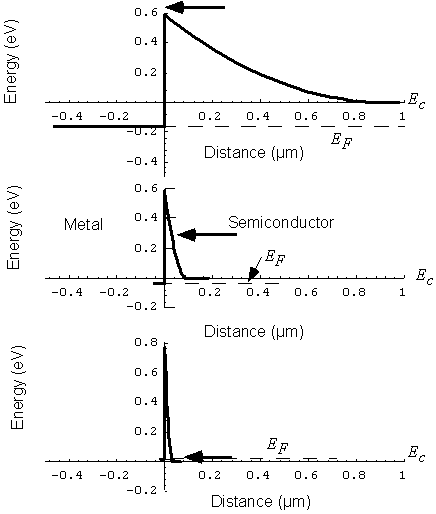
Fig.
4. Band diagrams of Schottky barrier junctions for GaAs for doping levels Nd =
1015
cm–3 (top graph),
Nd =
1017
cm–3 (middle graph),
and Nd =
1018
cm–3 (bottom
graph). Arrows indicate electron transfer across the barrier under
forward bias. At very low doping levels, electrons go over the
barrier closer to the top of the barrier (this process is called thermionic emission). At moderated doping
levels, electrons tunnel across the barrier closer to the top of the
barrier (this process is called thermionic-field
emission). In highly doped degenerate semiconductors, electrons near
the Fermi level tunnel across a very thin depletion region (this process
is called field emission).
The current-voltage
characteristic of a Schottky diode in the case
of thermionic-field emission can be calculated
using the same approach as for the thermionic
model, except that in thermionic-field emission
case, we have to evaluate the product of the tunneling transmission
coefficient and the
number of electrons at a given energy as a function of energy and
integrate over the states in the conduction band. Such a calculation [see Rhoderick and Williams (1988)] yields the following
expression for the current density in the thermionic-field emission regime under forward
bias:
 (15)
(15)
where
 (16)
(16)
 (17)
(17)
 (18) (18)
In GaAs Schottky diodes, the thermionic-field emission becomes important
for Nd > 1017
cm–3 at 300 K and for
Nd > 1016
cm–3 at 77 K. In silicon, the corresponding values of
Nd are several times
larger. The forward j-V characteristics are shown in Fig.
5.

Fig. 5. Forward j-V
characteristics of GaAs Schottky diodes doped at 1015,
1017, and
1018
cm–3 (curves are
marked accordingly) at T = 300 K.
The
resistance of the Schottky barrier; in the field emission regime is quite
low. Therefore metal-n+ contacts are used as ohmic contacts. The specific contact resistance,
rc,
decreases with the increase in the doping level of the
semiconductor. (This resistance may vary from 10-3
Ωcm2 to 10-7 Ωcm2 or even
smaller depending on semiconductor material, doping level, contact metal,
and ohmic contact fabrication
technology.)
A Schottky diode
is a majority carrier device, where electron-hole recombination is usually
not important. Hence, Schottky diodes have
a much faster response under forward bias conditions than
p-n junction diodes. Therefore, Schottky diodes are used in applications where the
speed of a response is important, for example, in microwave
detectors, mixers, and varactors.
Prof. Dojin Kin site
OHMIC CONTACTS
In the case of a p-n diode, for
example, contacts have to be provided to both p-type and
n-type regions of the device in order to connect the diode to an
external circuit. These contacts have to be as unobtrusive as
possible, so that the current flowing through a semiconductor device and,
hence, through the contacts, leads to the smallest parasitic voltage drop
possible. Whatever voltage drop does occur across the contact has to
be proportional to the current so that the contacts do not introduce
uncontrollable and unexpected nonlinear elements into the circuit.
Since such contacts satisfy Ohm's law, they are usually called ohmic contacts.
As was discussed, a contact between a metal
and a semiconductor is typically a Schottky
barrier contact. However, if the semiconductor is very highly doped,
the Schottky barrier depletion region
becomes very thin, as illustrated in Fig. 4. At very high doping
levels, a thin depletion layer becomes quite transparent for electron
tunneling. This suggests that a practical way to make a good ohmic contact is to make a very highly doped
semiconductor region between the contact metal and the
semiconductor.
It may have been better to use a metal with
a work function, Fm, which is equal to or
smaller than the work function of a semiconductor, Fs. However, for most
semiconductors, it is difficult to find such a metal acceptable for
practical contacts.
Current-voltage characteristics of a Schottky barrier diode and of an ohmic contact are compared in Fig. 1. As
was mentioned above, a good ohmic contact should
have a linear current-voltage characteristic and a very small resistance
that is negligible compared to the resistance of the active region of the
semiconductor device. An ohmic contact with the
I-V characteristic shown in Fig. 2 does not satisfy fully these
conditions since the voltage drop across this contact is not negligibly
small compared with the voltage drop across the Schottky diode at moderate current densities above 0.1 kA/cm2.
As was discussed, the barrier between a
metal and a semiconductor is usually smaller for semiconductors with
smaller energy gaps.Hence, another way to decrease the contact resistance
is to place a layer of a narrow gap highly doped semiconductor material
between the active region of the device and the contact metal. Some
of the best ohmic contacts to date have been
made this way.
A quantitative measure of the contact
quality is the specific contact resistance, rc, which is the contact
resistance of a unit area contact. Depending on the semiconductor
material and on the contact quality, rc can vary anywhere from
10-3 Ωcm2 to 10-7
Ωcm2 or even less.
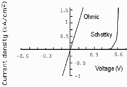
Fig. 1. Current-voltage characteristics of
ohmic and Schottky
barrier metal-semiconductor contacts to GaAs. (Schottky
contact is to GaAs doped at 1015
cm-3.) Ohmic contact resistance is 104
Ωcm2.
Most semiconductor devices have either a
sandwich structure or a planar structure, as illustrated in Fig.
2. The contact resistance of each contact in a sandwich structure
contact is given by
 (1)
(1)
A typical current density in a sandwich
type device can be as high as 104 A/cm2.
Hence, the specific contact resistance of 10-5 Ωcm2 would lead to a voltage drop
on the order of 0.1 V. This may be barely
acceptable. A larger specific contact resistance of
10-4 Ωcm2 or so would definitely lead
to problems, as we can see from Fig. 1.
These estimates
show that a semiconductor material can become viable for applications in
electronic devices only when good ohmic contacts
with low contact resistances become available. Often, poor ohmic contacts become a major stumbling block for applications of new semiconductor
materials.
|
![]() Programm
Programm ![]() Quant.mech.Intro
Quant.mech.Intro
![]() Sol.St.Intro
Sol.St.Intro
![]() defects
defects ![]() quant.structures
quant.structures ![]() auto-organization
auto-organization
![]() p-n
structures
p-n
structures ![]() schottky structures
schottky structures ![]() hetero structures
hetero structures
![]() photodetectors
photodetectors
![]() Light-emitters
Light-emitters ![]() transistors
transistors ![]() Technology
Technology ![]()
![]()


 is the Richardson constant and fB is the Schottky barrier
height.


![]() (
(![]() (2)
(2)![]() (3)
(3)![]() (4)
(4)![]() (
(![]() (
( (
( (a)
(b)
(c)
 (
( (
(![]() (
( (
( (
( (
( (
(
 (
( (16)
(16) (17)
(17) (18)
(18)


![]() (
(