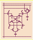
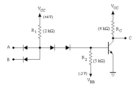
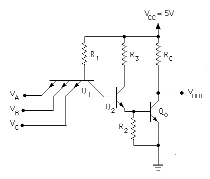
Electronic Devices and Circuits
Engineering Sciences 154

An Introduction to Digital Logic Familities

In the beginning (almost) there was diode logic (DL).reference

See a beautiful little DL Demonstrator (local copy) from HyperPhysics
Level-Shifted Diode Logic Two-Input NAND Gate
  • With either input at 0V,
    Vx=0.7 V, DL is just cut off,
    and VOUT = 0 V.
     
  • With both inputs at 1 V,
    VX=1.7 V and VOUT=1 V.

Then there was resistor-transistor logic (RTL)....

Resistor-Transistor Logic
Two-Input NOR Gate
Two-Input NAND Gate

and diode-transistor logic (DTL).

 A Diode-Transistor Logic (DTL) Two-Input NAND Gate
  • If all inputs are high, Vx = 2.2 V and
    the transistor is saturated.
  • If any input goes low (0.2 V), Vx = 0.9 V
    and the transistor cuts off.
     
  • The added resistor R2 provides a discharge
    path for stored base charge in the BJT, to
    provide a reasonable L->H transition time.
 930 Series Diode-Transistor Logic Three-Input NAND Gate

Which begat transistor-transistor logic (TTL).

Basic Transistor-Transistor Logic (TTL) Inverter
Basic Multi-emitter TTL Three-Input NAND Gate
   ALL INPUTS HIGH.
ï Q1 is reverse active.
ï QO is saturated.
ï VOL = VCE(sat)
  ANY INPUT LOW.
ï Q1 is saturated.
ï QO is cut off.
ï VOH = VCC
TTL Switching or Transistion Times
(see illustration)
    Low to High Transistion
  • The time required to discharge the Q1 depletion layers is << 1ns.
     
  • The time required to extract the Q2 base charge is also << 1ns:
    • Q1 becomes forward active;
    • IBR becomes large for Q2
  • Removal of base charge from QO is similar to the DTL case.  With R2 = 1 kW, ts = 10ns (typical values for 7400 series TTL).
    High to Low Transistion
  • The depletion capacitance of the Q1 EB junction must discharge;
     
  • Base charge must be removed from the saturated Q2
     
  • Ditto for QO
     
  • The capactive load must be charged to VCC.


Low-Power Schottky TTL (74LS Series)

    Click on image to enlarge
  Why go back to DTL?
  • The Schottky diodes can be made smaller than Q1, with lower parasitic capacitances, with post 1975 technology (6mm features).
     
  • QS can not saturate, so it is not neccessary to remove its base charge with a BJT.


CMOS and NMOS Logic

See our MOS logic page

References

See notes from Professor John Emerson Ayers course on
Digital Integrated Circuits particularly the notes on DTL/TTL (local copy).

See also Inside Logic Gates


This page was prepared and is maintained by R. Victor Jones
Comments to: mailto:%20jones.deas.harvard.edu.
Last updated December 11, 2001