The purposes of this project are the
integrated system of the micro optoelectronic components
such as the blue laser diode pick-up head, the know-how
of the high frequency microwave and the optoelectronic
element integrated circuits, and the advance techniques
for the new trend in the next century. We hope that
we can establish the fabrication techniques of the
silicon wafer, the gallium arsenide high frequency
devices, and the optoelectronic element. We integrate
and make use of the specialties of the research
teams in the national central university, in order
complete a sophisticated project of crossing over
several academic researches. Then we can upgrade
to the level of the advanced countries for the research
of the integrated micro optoelectronic system in
our country, and we expect that we join in the international
top research communities. This “integrated micro-optoelectronics
devices and systems” research project consists of
2 sub-projects:
1. The techniques of Micro-Optoelectronics
2. High frequency microwave and optoelectronic integrated
circuit system
This interdisciplinary project will be executed
by a research group containing 11 professors of
different research domains. They come from institute
of optical science, electrical engineering department,
mechanical engineering department and physics department
of National Central University We will also invite
Pr. Ming C. Wu of UCLA and Pr. Ming Fon of university
of Illinois as consultants.
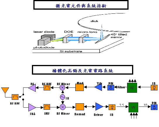
The purpose of the first sub-project is to build
the micro-optoelectronic technique. It is not only
to build the micro-optical parts such as micromirror,
microlens, and etc, but also to integrate them together
to a system. In this project, the micro-optical
bench and the next generation blue laser DVD pickup
head will be developed.
This propose is to develop the micro-optical
techniques, including:
(1) Manufacture technique for micro-optical parts.
(2) Wafer bonding or chip bonding, to put micro-optical
parts bond together when building in different
substrate.
(3) Integration technique to assemble the micro-optics
parts into system.
The major task of the second sub-project is to
explore the III-V compound semiconductor (GaAs,
InP and GaN) based materials, devices (high-speed
electronics and optoelectronics), and integrated
circuit for modern communication system, which
include wireless communication and optical fiber
communication.
To establish the ability of 0.1μm fabrication
is the starting point for this whole project.
Base on this 0.1μm fabrication ability, the processing
technique, design and integration for a high operation
frequency (f>30GHz) integrated circuit will
be developed. The development covers (1) RF transceiver
based on III-V (GaAs and InP) compound semiconductor.
(2) Silicon monolithic integrated circuit for
RF application.
On the other hand, the development of optical
fiber communication for 10Gbps includes the starting
point of 0.1μm fabrication ability, GaN-based
quantum dot blue laser, III-V compound based drive
circuits, photo-detector and amplifiers.
Since transistors invented in 1947 and the mature
of integrated circuits technologies, modern electronic
system has been approached to a new era of “system-on-a-chip”.
Those two communication systems will finally be
integrated on silicon substrate with other silicon
based circuits (other projects) to achieve this
concept: “system-on-a-chip”.
|