| |
 |
 |
|
| .The
project Results |
 |
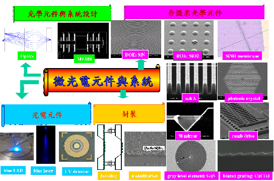
◎The techniques
of Micro-Optoelectronics: |
The purpose of this project is the
development of micro-optoelectronic techniques,
and it is based on the research of optoelectronic
semiconductor material, manufacturing process, the
optical design, optical system and the diffraction
component etc. in national central university. Then
the development can be extensible further again,
and make us can reach top-grade and outstanding
level. This project not only wants to develop manufacturing
techniques of the micro-optoelectronic components,
such as semiconductor laser, semiconductor detector,
micro-mirror, micro-lens, the beam splitter and
DOE( the Diffractive Optical Element) etc., and
we assemble all the optics electrical element on
the same chip, and the various subsystems in different
substrate are made together with the wafer bonding
technique, that can increase the miniaturization
and functionalities of the micro-optoelectronic
system. We use the next generation blue laser pick-up
head as a carrier to develop the integrated silicon
micro-optical bench, the development of the high
speed and the high frequency electric circuit system,
and the bonding system of the silicon micro-optical
bench. Besides the existing researches for the micro-optoelectronic
techniques, it also includes:
(1) Manufacture technique for micro-optical parts.
(2) Wafer bonding or chip bonding, to put micro-optical
parts bond together when building in different substrate.
(3) Integration technique to assemble the micro-optics
parts into system.
|
|
The executed item of
this project has:
(A)
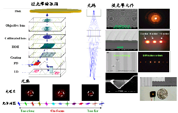
Optical system
The optical components of the optical pick-up head
are an off-axis for the planar type, and they are
on-axis for the free space system. Therefore, each
component is hard to manufacture because of being
limited by the manufacturing processes. Then it
needed to feed back to the design for making an
improvement. The waveguide type was another a kind
of design, it can make the splitting grating and
the coupling grating on same plane waveguide, so
they can be aligned on the same time to avoid the
packaging problems.
(B)
The optical components and special optical components
|
- Microlens: We will make a lens on the substrate
by using ICP, to get a selectivity of 1:1 (photo-resist:
substrate) by changing the parameters of chemistry
and plasma etc..
- The design of the high NA lens: We will try
to enlarge the curvature of microlens to reduce
its focal length, and raise its NA; Also we
will integrate two lenses together, to raise
its NA.
- The manufacture and the measurement of the
High-NA GaN DOE microlens: We will fabricate
high-NA GaN diffractive microlens by the gray
level photomask and the ICP etching technique,
and to measure its optical properties including
the influence analysis of the optics field to
focusing due to the error of manufacturing processes,
and the noise analysis of the environment. The
FWHW of the optical field for focusing was 0.3
um by theoretical calculating. It is suitable
for the application of next generation DVD systems.
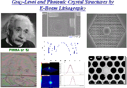
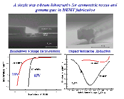
- Manufacture of the concave micro-mirror by
the e-beam lithography: We will fabricate the
micro-mirror on the silicon by using the e-beam
lithography, and it is 1 um for the height of
the concave micro-mirror.
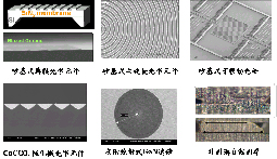
- Polarization sensitive element: Continue,
the CaCO3 of Etching of 1 mm structure: For
enhancing the optics efficiency of the optical
pick-up head, we develop a birefrigent crystal
with the index matching technique, to get an
anisotropic etching by reducing the width to
be 3 mm. Also we want to develop the sub-micro
technique for getting the polarization sensitive
phase, then we can made the polarization sensitive
optical component.
- The e-beam direct writing and a subwavelength
optical component: The width below 0.5 μm for
the subwavelength structure, it is needed the
technique of the e-beam direct writing. We will
fabricate a subwavelength structure on the silicon,
the goals are to make a 1/4 waveplates, the
gray-level lens and polarization sensitive components.
- Gray-level optical components: We make a
gray-level mask on the top of LDW glass by using
the laser direct writing, and to fabricate gray-level
optical components. We will integrate the laser
direct write system, including optical alignment,
monitoring, intensity control, focusing, precise
movement system, to make the pattern of grating
and lens can be directly written on the photomask
glass; Again, we will expose the patterns on
the photo-resist by photolithography, then we
can get a pattern on the substrate by 1:1 selectivity
etching.
|
|
| (C)
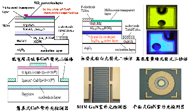
The development of the GaN photodiode: |
- The manufacture of the cutoff wavelength as
405± 5 nm GaN detector to be matched with the
application of the blue violet optical pick-up
head.
- The manufacture of the GaN detector that
its transient response time can be the ns order.
|
|
(D)The
technique of combining the micro optical components
and the microelectronics components on the micro
optical bench:
We will use the silicon material to be a substrate
to get a trench on the micro optical bench by
using the ICP deep etching, and insert them into
the micro optical bench one by one. The position
of component's can be defined on the optical bench
by the photolithography and the ICP etching. The
diameter of the optical fiber is more precise(125
±s 1 um), and its diameter dimension is suits
for micro system, and can be operated by a hand.
So it can be used in MEMS for the alignment of
micro optical components. |
|
(E)The
design and fabrication of MEMS chips:
We will finish the works in the last year that
is removing the sacrifice layer on the chips by
the HF solution, and developing the technique
of lifting and lodging the optical components
on the bench. We will renew the design after analyzing
this merit of this chips, and carry on the design
of actuator.
(F) Cooling of
small hot spot:
The cooling of the small hot spot, for example
the small hot spot cooling of the blue laser,
the quantum well laser and the quantum dot laser
etc., is not good in regard to the present techniques.
Currently, there are still unmanned development
and no real small hot spot equipments. This project
has already completed with a small hot spot experiment
that cooling of 50μm by 50μm directly, and approach
to the design and the manufacturing techniques
for integration. |
| |
| ◎The techniques
of Micro-Optoelectronics: |
Since transistors invented
in 1947 and the mature of integrated circuits technologies,
modern electronic system has been approached to
a new era of “system-on-a-chip”. The major task
of the second sub-project is to explore the III-V
compound semiconductor (GaAs, InP and GaN) based
materials, devices (high-speed electronics and optoelectronics),
and integrated circuit for modern communication
system, which include wireless communication and
optical fiber communication.
To establish the ability of 0.1μm fabrication is
the starting point for this whole project. Base
on this 0.1μm fabrication ability, the processing
technique, design and integration for a high operation
frequency (f>30GHz) integrated circuit will be
developed. The development covers
(1) RF transceiver based on III-V (GaAs and InP)
compound semiconductor.
(2) The design and fabrication of Ka band integrated
circuit.
On the other hand, the development of optical fiber
communication for 10Gbps includes the starting point
of 0.1μm fabrication ability, GaN-based quantum
dot blue laser, The development covers
(1) The design and integration of the laser and
driver circuit based on III-V (GaAs, InP, and GaN)
compound semiconductor.
(2) The design and integration of photo-detector
and amplifiers.
Those two communication systems will finally be
integrated on silicon substrate or Al2O3 with other
silicon based circuits (other projects) to achieve
this concept: “system-on-a-chip”. |
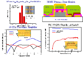
| (A)high
frequency FET and the design of mm waves circuit
|
- The fabrication of 0.1-0.15 μm T gate heterostructure
FETs on GaAs substrate by using e-beam lithography.
- Measuring the DC and RF performance of this
0.1-0.15μm FETs, and establishing the high-frequency
large signal model of this device for the design
of mm wave integrated circuit.
- Design and fabrication of the transmission
line operating in 30-60 GHz, and set up its
model.
- Design of the amplifier, oscillator, multiplier
and mixer for operating in 30 GHz.
- Fabrication of 0.2 microns MSM photo-detector,
to make it operating frequently widely and exceed
10 Gbps.
- The design of pre-amplifier and restriction
amplifier for optical communication by using
0.15 μm FETs
- The development of 50nm array in order to
apply for the design of patterned quantum dots.
- The development of 50nm array in order to
apply for the optics gratings, and the photonic
crystal.
|
| Key working project and
Technical indicator |
- 0.15um T-gate GaAs based pHEMT fT>60GHz,fmax>90GHz
- Power Device Fabrication Pout>15 dBm at
28 GHz
- Device Nonlinear Modeling IV, Power,IP3
- Coplanar Passive Component Design Transmission
Line
- GaAs based pHEMT amplifier Pout>15 dBm
- GaAs based pHEMT LNA Gain>10dB,NF<3dB
|
|
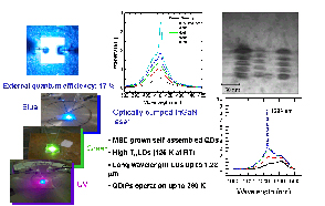
| (B)
The HD-DVD laser diode and the growth of GaN quantum
dots structure |
|
|
- The optimizations of laser structure include
the thickness of covering layer, composition,
the numbers of multi quantum well, width of
quantum well, and the doping concentration
etc. They can be the optimization references
of the laser structure according to the measurement
and analysis of the laser far field.
- It can reduces the defect density of Ga(Al)N
material by using the PENDEO method, to enhance
its life time. We also study the inferior
mechanism through the measurement of electricity
and TEM, to be the tool for enhancing the
performance of the devices.
- The fabrication processes of laser diode
include the low resistivity and high thermal
stability of the ohmic contact. The laser
resonant cavity need to be optimized, and
the reflectivity of laser mirror can be enhanced
by the technique of the high reflectivity
mirror, then we could reduce the threshold
current of the laser.
|
- The growth of GaN quantum
dots structure:
|
- We grow the quantum dots of InGaN, or GaN
through the stress effect of the Stranski-Krastanov
method.
- We can get quantum dots structure through
the 3D growth of InGaN by using the doping
of Si, or Mg as Anti-surfactant.
- We can control the uniformity and density
of quantum dots through the selective growth
by using the mask of the SiO2 or SiNx.
- We can measure the shape, dimension, density
and the crystal structure by using the AFM
and TEM to compute the energy level of the
quantum dots, and compare with the results
of PL. We will also discuss the carrier transition
affected by the piezoelectric effect.
|
|
| (C)The
hetero-structure bipolar transistors and the fabrication
of electric circuit |
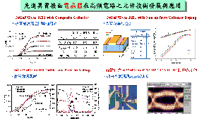
- The application of
analog circuit:
|
The main application is the Ka-band power amplifier.
The key development will complete the power
transistor and the related passive RF devices
(the CPW devices).The technique of devices is
mainly based on the InP-based DHBTs and the
InGaP/GaAs DHBT, and use the composite collector
of the InGaAsP materials and the high concentration
InP, and add the following expitaxy layer between
base-collector to improve DEC: InGaAs(150 As,
undoped), InGaAsP(undoped), InP.(150 As,3'1017
cms-3s)
|
- The application of
digital circuit:
|
The main appplied object is a 40 Gbs/s high-speed
fiber-optic communication. The techniques of
these devices are mainly based on the InP-based
SHBTs. We grow the InP series HBT by MBE firstly,
then they are taking into a manufacturing processes.
In order to fit the high frequency request of
Ka-band, the whole processes has to shrink the
width of emitter to be 1 μm and add the process
of the air-bridge for connecting. The manufacturing
process firstly describes as follows:
|
- ISO (light field): definition of devices,
BCB planization
- EMI (dark field): emitter area definition
and emitter metal metallization
- BAS (dark field): base contact metallization
- MES (light field): base-collector junction
definition
- COL (dark field): collector contact metallization
- VIA (dark field): via opening on to emitter,
base, and collector contacts
- ME1(dark field): Au plating for air-bridge
- PAD(dark field): microwave pads definition
|
We will carry on the above-mentioned first
manufacturing process for obtaining a good mesa
of devices , and have to adopt the dry etching
to avoid an inclined rate of wet etching. This
etching will carry out by using the High Density
Plasma Etcher of Unaxis 860L that can accurately
monitor the etching layer with the endpoint
detector.
|
|
| (D)The
study of Si waveguide and the passive component
for the application of DWDM |
| In the this subproject, we will develop
the technique of the Si waveguide based on SOI structure
and the passive component used in DWDM. We will
use the BPM method for the foundation design of
the Si waveguide and the optics coupler in this
year. We will develop a technique by E-beam lithography
to remove the phenomenons of the arched acute angle
and the stuck narrow angle due to the expose and
develop for the fabrication processes, and use a
dry etching technique of the high density plasma
to make the edge of the waveguide is smooth and
vertical, then fabricate the low loss transmission
and low cross talk of the silicon waveguide component.
We will design and fabricate the Si array waveguide
grating (AWG) by the results of the silicon waveguide. |
| (E)The
packaging of micro optical components and the wafer
bonding |
| The purpose of this subproject is
to purchase a wafer bonder, and complete the technique
development of this wafer bonder. After reaching
the technique level of wafer bonding in the world,
we will toward to break through the existing techniques,
and develop the new technique for the first goal
of the next stage. |
|
|
|